Browse categories
English
$
USD
Connect to your AI
PCB Layout Designer KiCad Altium Custom PCB Design Specialist
Is your electronic product too complex for a standard two-layer PCB?
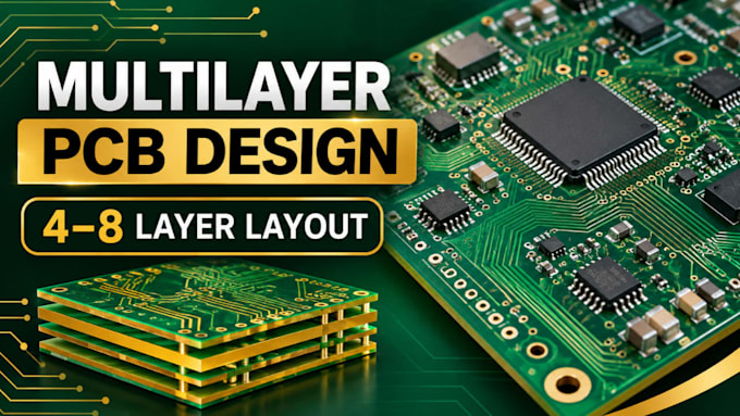
I will design a professional multilayer PCB layout for your complex electronic product, helping you organize components and routing across multiple copper layers based on your supplied schematic and technical requirements.
My multilayer PCB design service includes:
- 4-layer, 6-layer and other agreed multilayer PCB layouts
- Component placement and PCB routing
- Power and ground plane arrangement where required
- PCB layer stack-up implementation based on project requirements
- Design Rule Check (DRC)
- Gerber and drill files
- Bill of Materials (BOM)
- Editable PCB source files
- 2D and 3D board views where supported
I work from your supplied schematic, component information, board dimensions and manufacturing requirements.
Please note: This service covers PCB layout and design documentation. Circuit invention, firmware development, physical manufacturing and assembly are not included. Advanced signal-integrity, impedance-control and high-speed validation services must be agreed separately.
Contact me before ordering so I can review your layer count, board complexity and deliverables.