Browse categories
English
$
USD
Connect to your AI
Hardware Design Engineer PCB Firmware And IoT Development
HELLO AND WELCOME
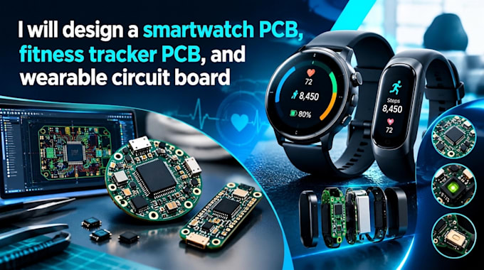
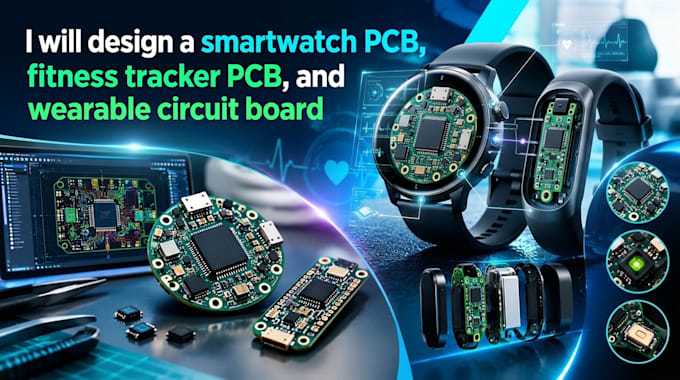
Looking for a professional PCB designer for your smartwatch, fitness tracker, or wearable electronics project?
I will design a compact reliable and efficient wearable PCB tailored to your requirements.
My services include:
I focus on quality, efficient power usage and manufacturing ready PCB designs.
Why work with me:
Contact me before ordering to discuss your project and choose the right package. Let's bring your wearable electronics idea to life!

Specialization:
Circuit design
•
Schematics
•
Layout
•
Analysis
•
Gerber
File format:
Gerber
•
STEP
•
BRD
•
•
Pcbdoc
Software:
Altium Designer
•
Eagle CAD
•
EasyEDA
•
KiCad
Interface:
I2S
•
UART
•
USB
•
SPI
•
BLE
•
BT
Can you design a PCB for a custom smartwatch prototype?
Yes. I can help design a custom smartwatch PCB based on your required features component selection board dimensions connectivity and power requirements.
Can you modify or improve my existing wearable PCB design?
Yes. I can review your existing schematics or PCB layout and help improve component placement, board dimensions, power efficiency, and design quality within the agreed scope
Can you help me choose components for my wearable PCB?
Yes. I can help select suitable microcontrollers, sensors, power components, and wireless modules based on your device functionality, size constraints, power budget, and project budget.
Can you design a compact, low-power PCB for my wearable device?
Yes. I can optimize the PCB layout for compact dimensions component placement and power efficiency, depending on your device requirements and design constraints.