Browse categories
English
$
USD
Connect to your AI
Pcb designer
HELLO AND WELCOME!
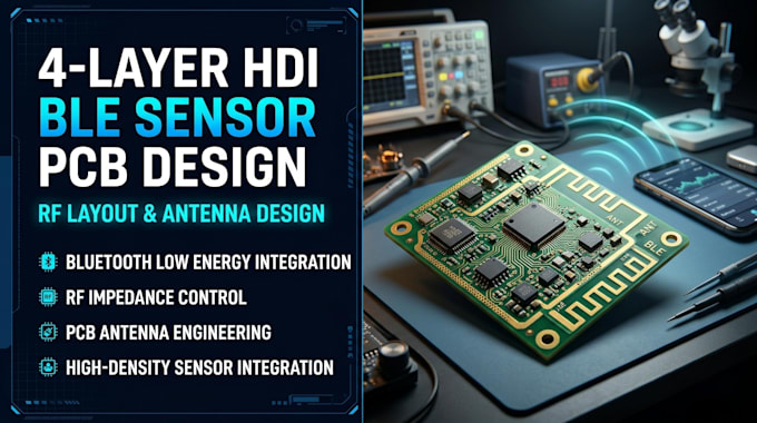
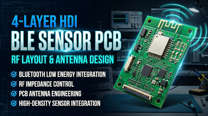
Designing a compact BLE-enabled sensor device requires more than fitting components onto a small PCB. It demands careful control of RF impedance, antenna radiation characteristics, high-speed signal integrity, power distribution, and electromagnetic interference to maintain reliable wireless communication within a limited board footprint.
What I Will Provide;
Why Choose Me?
Ready to build a compact, high-performance wireless sensor device? message now Let's engineer your 4-layer HDI BLE PCB with optimized RF routing, reliable antenna integration, and low-power architecture!!!.



Can you design a complete 4-layer HDI BLE sensor PCB?
Yes. I can develop the schematic, stack-up, component placement, RF routing, antenna integration, and manufacturing files.
Can you integrate Bluetooth Low Energy modules?
Yes. I can integrate BLE SoCs and modules from manufacturers such as Nordic Semiconductor, Silicon Labs, and Espressif, depending on project requirements.
Do you support custom PCB antenna design?
Yes. I can develop PCB antenna layouts and integration structures based on the selected frequency band, board dimensions, and RF requirements.
Can you design controlled-impedance RF traces?
Yes. I can plan RF transmission lines using the PCB stack-up, dielectric properties, copper thickness, and target impedance.
Can you integrate multiple sensors?
Yes. I can integrate environmental, motion, pressure, temperature, and other compatible sensor interfaces.
Do you support low-power BLE applications?
Yes. I can optimize the hardware architecture for reduced power consumption, battery operation, and efficient wireless communication.
Will you provide manufacturing files?
Yes. I can provide Gerber files, BOM, schematics, PCB layout files, and assembly documentation.
Can you review and improve an existing RF PCB?
Yes. I can review your existing layout, identify potential RF and signal integrity issues, and recommend improvements.