Browse categories
Explore
Fiverr Pro
English
$
USD
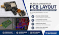
3D Rendering, Weld Drawing and RF PCB Layout One Engineer, Full Delivery
RF and flex PCB layout requires precision beyond standard design rules. Improper antenna routing detunes signals, poor flex design causes mechanical failure, and incorrect rigid-flex stackups break signal integrity at transition zones.
I design RF, flex, and rigid-flex PCBs in Altium or KiCad with controlled impedance, antenna routing, and proper mechanical constraints for reliable real-world performance.
I OFFER:
YOU GET:
Message me with your frequency, stackup, and requirements before ordering.

Do you design RF and high frequency PCB layouts
Yes I specialize in RF high speed and controlled impedance PCB layouts including antenna design and signal integrity optimization
What software do you use
I use Altium Designer and KiCad for professional PCB layout stackup design and fabrication ready outputs
Can you handle flex and rigid flex PCB designs
Yes I design flex and rigid flex PCBs with proper bend radius transition zones and mechanical reliability
Will my PCB be fabrication ready
Yes you will receive clean fabrication ready Gerber files and all required manufacturing data
Do you provide source files
Yes Altium or KiCad source files are included depending on the project
Can you design antenna or wireless PCBs
Yes I design RF antenna layouts for WiFi Bluetooth and other wireless applications with impedance matching
