Browse categories
Explore
Fiverr Pro
English
$
USD
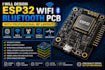
Electronics and PCB design specialist
I'm Edward white a professional reliable ESP32, WiFi, or Bluetooth PCB with proper RF performance?
I will design a high-quality PCB optimized for wireless communication, ensuring stable signal performance and manufacturability.
Whether you're building an IoT device, smart system, or prototype, I can help turn your idea into a ready-to-produce PCB
What I Offer
Why choose me?
What you will receive
Software I Use
CONTACT ME NOW LET START YOUR PROJECT TODAY

What do you need to start my project?
I need your circuit idea, block diagram, or requirements (features, size, power, etc.). If you don’t have a schematic, I can help design it from scratch.
Can you design RF PCBs for ESP32 WiFi/Bluetooth projects?
Yes, I design RF-aware layouts including proper grounding, trace routing, and antenna placement for stable wireless performance.
Do you provide manufacturing files?
Yes, I provide Gerber files, drill files, BOM (Bill of Materials), and pick-and-place files ready for fabrication.
Can you work with existing designs?
Yes, I can improve, fix, or optimize your existing PCB for better RF performance and reliability.
