Browse categories
Explore
Fiverr Pro
English
$
USD
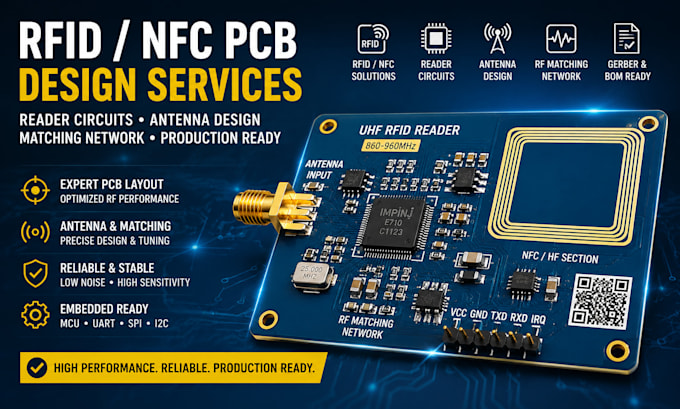
Building an RFID or NFC product? I design PCB layouts around your reader IC, antenna and interface requirements.
WHAT I CAN DO
BENEFITS YOULL GET:
Receive a clear design package tailored to your target frequency, chip datasheet, board size and use case. Ill flag missing information early, explain key design decisions and confirm deliverables before work begins.
TOOLS I WORK WITH:
KiCad or Altium Designer, depending on your own project.
IDEAL PROJECTS:
Send your reader IC, target frequency, antenna dimensions, schematic or reference design, board outline and manufacturer requirements.
Contact me first for complex UHF systems. Read range depends on the final enclosure, antenna environment and physical testing; lab tuning and certification are excluded unless agreed.


Can you design an RFID or NFC PCB from scratch?
Yes, when the project requirements and supported components are clearly defined. Please send your application, reader IC, target frequency and available reference designs so I can confirm the scope.
Can you work with PN532 or MFRC522?
I can work with supported reader ICs when the datasheet, interface requirements and design constraints are available. Share your exact part number before ordering.
Do you design NFC antennas and matching networks?
Antenna layout and matching-network design can be included where the required specifications and project scope are suitable. Final tuning may require prototype measurements.
What files will I receive?
Depending on your package, deliverables may include editable PCB and schematic files, Gerbers, a BOM and relevant manufacturing outputs. Confirm the exact deliverables before ordering.
Can you guarantee a specific RFID read range?
No layout alone can guarantee a specific read range. Results depend on antenna design, reader IC, enclosure, nearby materials, installation and testing. Physical validation is separate unless explicitly agreed.