Browse categories
English
$
USD
Connect to your AI
PCB Designer PCB Layout Schematic Design and Gerber Files
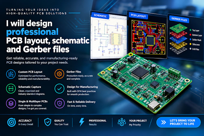
I will transform your electronic ideas into precision PCB layouts and manufacturing-ready files
Looking for a reliable PCB specialist to bring your electronics project to life? I help turn circuit concepts into practical, well-organized printed circuit boards with attention to detail, quality, and your project requirements
What I Offer
Why Choose Me
Whether you need a new PCB layout, schematic conversion, or manufacturing documentation, I am ready to help turn your ideas into practical electronic solutions.
File format:
Gerber
•
STEP
•
SCH
•
Software:
Altium Designer
•
Eagle CAD
•
EasyEDA
•
KiCad
Interface:
UART
•
SPI
•
I2C
What information do you need to start my PCB design?
Please provide your schematic, circuit diagram, component list, project requirements, board dimensions, and preferred PCB layers if available. If you only have an idea, contact me to discuss your project before ordering.
What files will I receive after completing the project?
Depending on your selected package, you can receive Gerber files, drill files, schematic diagrams, a Bill of Materials (BOM), PDF previews, and editable source project files.
Can you design a PCB from an existing schematic?
Yes. I can create a PCB layout from your existing schematic, subject to project complexity and the information provided. Please share your files so I can review the requirements.
Do you provide PCB manufacturing and assembly?
My standard service focuses on PCB design and digital manufacturing files. Physical PCB fabrication, component sourcing, and assembly are not included unless agreed separately.
Can you modify an existing PCB design?
Yes. I can help modify an existing PCB layout, update components, improve routing, or prepare revised manufacturing files. Please provide the original editable project files and explain the changes you need.
