Browse categories
English
$
USD
Connect to your AI
HELLO THERE!
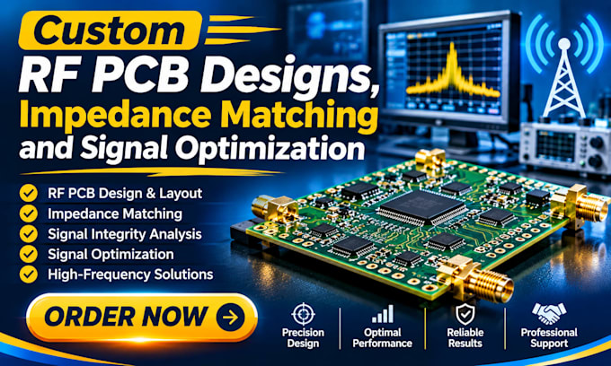
Need reliable RF PCB solutions with accurate impedance matching and optimized signal performance?
I provide professional RF engineering services for wireless electronics, high-frequency circuits and custom PCB projects.
My Services:
What Sets Me Apart:
I focus on precision, performance and reliability. Every project receives careful component selection, proper routing techniques and attention to RF requirements to achieve efficient signal transmission and minimize unwanted losses.
Whether you need a new RF board, an existing layout improved or help solving signal-related issues, I am ready to assist.
**Let's bring your RF electronics project to life. Contact me today to discuss your requirements and get started!



File format:
Gerber
•
STEP
•
VRML
•
BRD
•
SCH
Software:
Altium Designer
•
Eagle CAD
•
KiCad
•
AutoCAD
Interface:
I2S
•
UART
•
USB
•
SPI
•
I2C
•
Wi-Fi
•
Ethernet
What types of RF PCB projects do you handle?
I handle custom RF circuits, wireless communication boards, high-frequency PCB layouts and antenna-related projects.
Can you perform impedance matching?
Yes, I can calculate and optimize impedance matching for RF circuits and transmission lines.
Do you work with existing RF PCB layouts?
Yes, I can review, modify and improve existing layouts to enhance signal performance.