Browse categories
Explore
Fiverr Pro
English
$
USD
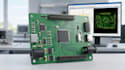
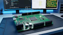
Welcome to my RF PCB Design Service.
Are you looking for a professional RF PCB designer for your wireless communication, IoT, antenna, or radio frequency project? I will design high-quality RF circuit schematics and RF PCB layouts optimized for performance, signal integrity, impedance control, low noise, and manufacturability.
I specialize in RF schematic design, multilayer PCB layout, RF routing, antenna matching networks, RF amplifier and filter circuits, component placement optimization, and complete production-ready PCB files. I ensure proper grounding, controlled impedance, and efficient RF performance for reliable operation.
You will receive complete design outputs including schematic files, PCB layout files, Gerber files, BOM, pick and place files, and documentation ready for fabrication.
Why choose my service:
Please contact me before placing an order to discuss your project requirements for the best results.

1. What RF frequencies do you support?
I can design RF circuits for low-frequency, ISM band, WiFi, Bluetooth, GPS, LoRa, GSM, LTE, and other wireless communication applications.
2. What files will I receive?
You will receive schematic files, PCB layout files, Gerber files, BOM, pick and place files, PDF documentation, and manufacturing outputs.
3. Can you redesign or improve an existing RF PCB?
Yes. I can review, optimize, troubleshoot, and redesign existing RF circuits and PCB layouts for better performance.
4. Do you provide antenna integration?
Yes. I can assist with antenna matching networks, RF routing, and antenna placement considerations.
5. Which PCB software do you use?
I work with Altium Designer, KiCad, EasyEDA, Eagle, and other professional PCB design tools.


