Browse categories
Explore
Fiverr Pro
English
$
USD
Senior PCB Design Engineer
I design PCB layouts that are ready for fabrication and assembly.
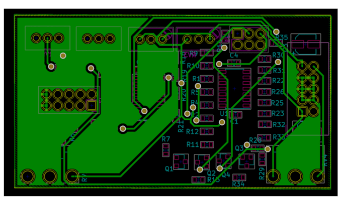
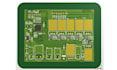
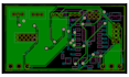
If you have a schematic, I will convert it into a properly routed PCB with correct stackup, grounding, and signal flow. The focus is on electrical performance and manufacturability, not just visual layout.
Services:
I work on microcontroller boards (STM32, ESP32, Arduino), embedded systems, and mixed-signal designs.
Send your schematic, board size, and layer count before placing an order.
What do you need to start the PCB design?
I need your schematic (PDF or source file), board dimensions, layer count, component list if available, and any mechanical constraints.
Can you design PCB from just an idea or block diagram?
No. I only work from a completed schematic. If you don’t have one, you must provide full circuit details first.
Which software do you use?
Altium Designer, KiCad, or Eagle depending on the project requirements.
Do you provide fabrication files?
Yes. I deliver Gerber files, drill files, BOM, and pick & place files ready for manufacturing.
Can you handle high-speed or RF designs?
Yes, for moderate high-speed designs like USB, SPI, and differential pairs. RF projects depend on clear specifications.
Will the PCB be manufacturing-ready?
Yes, I follow DRC checks and basic DFM practices to ensure fabrication readiness.