Browse categories
Explore
Fiverr Pro
English
$
USD
ELECTRONICS AND ELECTRICAL ENGINEERING
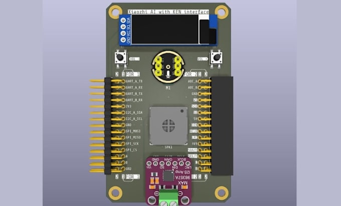
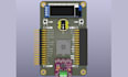
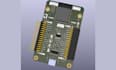
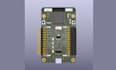
PCB design engineer experienced in multilayer PCB, high speed PCB, RF PCB, antenna PCB, and impedance controlled PCB deslgn. I create optimized, manufacturing ready circuit boards with a strong focus on signal integrity, EMI reduction, impedance matching, and reliable high frequency performance.
Whether you are developing wireless communication devices, IoT products, RF modules, embedded systems, automotive electronics, or advanced digital hardware, I can help transform your concept into a production ready PCB design.
What I Offer:
What You Will Receive:
Please contact me before placing an order so we can discuss your project requirements and determine the best solution for your deslgn.
What types of PCB projects can you handle?
I design multilayer PCB, high speed PCB, RF PCB, antenna PCB, impedance-controlled PCB, IoT devices, embedded systems, and communication hardware.
Can you design controlled impedance PCBs?
Yes. I can design controlled impedance traces, differential pairs, and optimized stackups for high-speed and RF applications.
Which PCB design software do you use?
I use KiCad, Altium Designer, and EasyEDA based on project requirements and manufacturing needs.
Will I receive manufacturing ready files?
Yes. You will receive Gerber files, BOM, pick-and-place files, source files, PCB stackup details, and fabrication documentation.
Can you review and optimize an existing PCB design?
Yes. I can analyze signal integrity, routing, impedance control, EMI concerns, and manufacturability to improve your design.
Do you design RF and high frequency PCBs?
Yes. I design RF circuits, antenna PCBs, wireless communication boards, and high frequency layouts with proper grounding, impedance matching, and routing practices.