Browse categories
Explore
Fiverr Pro
English
$
USD
PCB Design Specialist ,Circuit, Schematic and Layout
HELLO AND WELCOME!
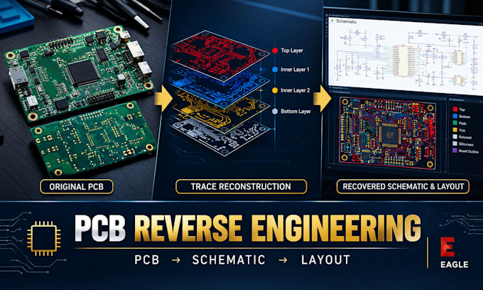
Do you have a PCB but no schematic, layout, BOM or original design files?
I will professionally reverse engineer your PCB and reconstruct the design into clean, editable engineering files for analysis, repair, modification, cloning or manufacturing.
I can work from clear PCB photos, physical boards, scans, existing Gerber files or available documentation.
My PCB reverse engineering services includes:
What i work with:
And other PCB design workflows,depending on the project requirements.
If you have an obsolete, damaged, undocumented or existing PCB, I will carefully analyze the available information and reconstruct the design.
Send me clear images of the top and bottom sides of your PCB before ordering. I will review the board complexity, layers and required deliverables and recommend the right package for your project.
Let's recover your PCB design and turn it into usable engineering files.
Can you reverse engineer a PCB from photos?
Yes. Clear, high-resolution images of both sides of the PCB can be used for an initial assessment. Additional information may be required for complex or multilayer boards
Can you recreate the schematic?
Yes. I can trace visible connections and recreate the circuit schematic based on the available PCB information
Can you recreate the PCB layout?
Yes, depending on the board, available information and required accuracy
Can you create Gerber files?
Yes, when sufficient design information is available to recreate the board properly.
Can you create a BOM?
Yes. I can prepare a Bill of Materials based on identifiable components and available markings/datasheets.
Can you reverse engineer multilayer PCBs?
Yes, subject to board complexity and the amount of information available. Please contact me before ordering for multilayer boards.
Can you work from an old or obsolete PCB?
Yes. PCB reverse engineering is particularly useful when original design documentation is missing or unavailable.
Do you provide editable files?
Yes, when included in the selected package.
Can you clone an existing PCB?
Yes. I can help recreate the design of an existing PCB for repair, modification, analysis or reproduction, subject to the available information and project requirements.