Browse categories
Explore
Fiverr Pro
English
$
USD
HELLO AND WELCOME!!
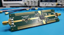
I will design professional RF PCB layouts, 50-ohm impedance-controlled routing, and RF circuit boards using KiCad, tailored to your project specifications and manufacturing requirements.
High-frequency PCB performance depends on more than component placement. Transmission-line geometry, return-current paths, ground-plane continuity, stack-up selection, and RF component positioning all influence signal integrity and circuit behavior.
What I Will Provide!!
Why Choose Me?
Message me today to discuss your RF PCB layout, 50 ohm routing, and RF circuit design requirements. Let's turn your concept into a manufacturing-ready design!

Can you design a 50-ohm controlled-impedance RF PCB?
Yes. I can design impedance-aware RF routing based on your target frequency, PCB material, copper thickness, dielectric thickness, and manufacturer stack-up information. Final impedance should be confirmed by the fabricator or appropriate validation.
Can you work with an existing RF schematic?
Yes. I can use your supplied schematic and component information to create a KiCad PCB layout, including placement, RF routing, grounding, and manufacturing outputs according to your selected package.
Which RF applications do you support?
I can support suitable RF layouts for Wi-Fi, Bluetooth, LoRa, GPS/GNSS, IoT wireless devices, RF transceivers, and other high-frequency circuits, depending on the project requirements.
Will I receive the KiCad files and Gerber outputs?
Yes. Native KiCad project files and manufacturing outputs can be included according to your selected package. BOM and additional documentation can also be provided when specified.
Do you provide RF simulation, antenna tuning, or physical testing?
These services must be agreed upon separately. A PCB layout alone does not guarantee RF performance, measured impedance, antenna efficiency, or regulatory compliance.


