Browse categories
Explore
Fiverr Pro
English
$
USD
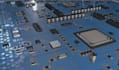
PCB LAYOUT AND DESIGN, INDUSTRIAL AND PRODUCT DESIGN
Looking for reliable pcb design that works perfectly the first time? I provide pcb layout, circuit, and schematic design ready for manufacturing with clean and accurate results.
Many struggle with failed boards, poor routing, and unusable gerber files. I help you avoid costly mistakes and deliver a pcb layout that is efficient, manufacturable, and reliable.
What you will get:
Tools :
Why Choose Me
Process:
Whether you need Pcb Designing for electronics, circuit, or schematic, this gig ensures quality results.
Message me before ordering to discuss your Project Details!

What do you need from me to start my PCB design?
I need a clear schematic or circuit diagram, list of components, and your board size requirements.
Can you design multilayer PCBs?
Yes, I can create multilayer PCB designs; please provide your layer count, components, and intended application.
Which software do you use for PCB design?
I use Altium Designer, KiCad, and EasyEDA; please specify if you have a preferred format or tool.
Will I receive Gerber files ready for manufacturing?
All packages include Gerber files; I just need your PCB specifications and intended manufacturer.
How many revisions are included?
Each package includes 2–5 revisions depending on the package; please provide detailed feedback for faster updates.
