Browse categories
Explore
Fiverr Pro
English
$
USD
Engineering Smart Circuits Automation And Wireless Innovation
Need professional RF PCB, microwave circuit, or antenna design and simulation?
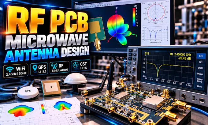
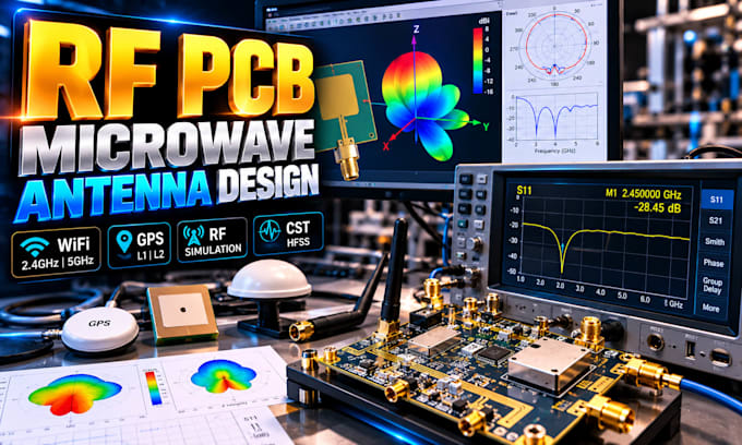
I provide RF engineering, RF PCB layout, microwave circuit design, antenna design, and electromagnetic simulation using CST Studio Suite, Ansys HFSS, Altium Designer, and KiCad.
Whether you're developing a WiFi, GPS, IoT, wireless communication, or high-frequency electronic device, I can help optimize your design for performance and manufacturability.
MY SERVICES INCLUDE:
WHY CHOOSE MY SERVICE?
Message me before ordering to discuss your frequency, specifications and project scope!



1: Can you design antennas for WiFi, GPS, 2.4GHz and 5GHz applications?
Yes! I can help with PCB antennas, microstrip antennas, patch antennas, and antenna arrays for wireless applications such as WiFi, GPS, IoT, and RF communication. Please share your operating frequency, bandwidth, gain, size, and other performance requirements.
2: Do you provide CST and HFSS simulation results?
Yes. Depending on the project, I can provide CST or HFSS simulation files, S-parameter plots, return loss, VSWR, radiation patterns, gain, and other relevant electromagnetic analysis results. The exact deliverables will be agreed upon before the order begins.
3: Can you design RF PCBs ready for manufacturing?
Yes. I can assist with RF PCB layout, controlled-impedance routing, component placement, PCB stackup planning, and manufacturing deliverables such as Gerber files, drill files, BOM, and source files. Fabrication requirements and substrate specifications should be confirmed before starting.
4: Can you improve an existing RF circuit or antenna design?
Yes. I can review existing RF circuits, PCB layouts, or antenna models and investigate issues such as poor impedance matching, return loss, bandwidth, coupling, and layout-related performance. Please provide your design files, specifications, and available measurement or simulation results.
5: Can you guarantee a specific antenna gain or RF performance?
I can design and optimize toward your target specifications, but final hardware performance depends on factors such as materials, manufacturing tolerances, connectors, enclosures, and real-world testing. Simulation results do not replace physical RF measurements and validation.