Browse categories
Explore
Fiverr Pro
English
$
USD
3D cad design expert, Product design expert and PCB Developer
Hi, Welcome to my Gig!
Are you tired of PCB designs that look good on screen but fail during assembly? Most buyers face the same headaches: signal interference, components that don't fit the enclosure, or files that manufacturing plants reject. You need a design that isn't just a layout, but a production ready solution.
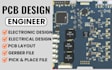
I design professional, optimized, and manufacturing ready PCBs for startups, engineers, students, and businesses using industry standard tools like KiCad, EasyEDA, Altium Designer, and Proteus.
What this gig:
Expertise: STM32 ESP32 Atmega Respbery Pi nRF
Tools I Use:
Send me your idea, schematic, or project requirements now, and lets build a high-quality PCB that works perfectly in the real world.

Do you provide manufacturing-ready PCB files?
Yes, I provide complete production-ready files including Gerber files, drill files, BOM, pick-and-place files, and 3D PCB views compatible with manufacturers like JLCPCB.
Can you design both schematic and PCB layout?
Absolutely. I can handle the complete process from schematic design to PCB layout, routing, optimization, and final manufacturing files.
Which PCB software do you use?
I work with industry-standard tools including Altium Designer, KiCad, EasyEDA, and Proteus depending on your project requirements.
Can you work on ESP32, STM32, Arduino, or IoT projects?
Yes, I specialize in embedded systems and IoT-based PCB designs using platforms like ESP32, STM32, and Arduino.
Will my PCB be checked for errors before delivery?
Yes. Every design goes through proper DRC (Design Rule Check), routing verification, and manufacturability checks before delivery.
Can you redesign or improve an existing PCB?
Yes, I can optimize, modify, or redesign existing PCB layouts for better performance, reduced noise, smaller size, or lower production cost.
Do you support multi-layer and RF PCB designs?
Yes, I design single-layer, double-layer, and multi-layer PCBs including RF, wireless, BLE, WiFi, and LoRa-based boards.
