Browse categories
English
$
USD
Connect to your AI
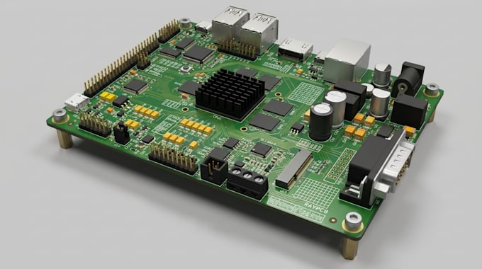
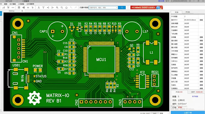
Professional ESP32 and USB C PCB Design, Reliable IoT Hardware
Is your wireless electronics project struggling to move from an RF concept to a properly designed PCB?
I develop custom RF PCB designs, LoRa circuit layouts and antenna integration solutions to help electronics developers organize their wireless hardware for prototyping and manufacturing.
From long range IoT devices and remote monitoring systems to wireless sensor networks and custom communication equipment, I approach each project according to its operating frequency, antenna requirements, board dimensions & intended application.
My services include RF PCB design with careful component placement and signal routing, custom LoRa board development for wireless communication and IoT applications & RF antenna integration with attention to antenna positioning, feed line routing and impedance matching.
I also can provide Gerber files, drill data, BOM & CPL files, alongside editable KiCad project documents for future modifications and development.
Message me now and let's give your wireless project a stronger foundation, from circuit layout to manufacturing preparation.
Can you design a custom RF or LoRa PCB from my project requirements?
Yes. I can develop a custom RF or LoRa PCB based on your application, operating frequency, circuit requirements, antenna specifications & preferred board dimensions.
Can you design and integrate an RF antenna into my PCB?
Yes. I can work on antenna integration, feed line routing and impedance matching considerations based on your selected frequency band and antenna requirements.
What manufacturing and assembly files will I receive?
Depending on your selected package, I can provide Gerber files, drill files, BOM, CPL component placement files and editable PCB design documents for fabrication and assembly preparation.
Can you improve an existing RF or LoRa PCB layout?
Absolutely. Send your existing KiCad files, schematic or PCB layout. I can check the design, identify potential layout issues & make agreed modifications to improve its organization and RF design considerations.