Browse categories
Explore
Fiverr Pro
English
$
USD
Hardware and IoT Specialist
Level 2
Has met high performance criteria and has a proven track record for meeting client expectations.
Most PCB designers hand you a routed board and walk away. I hand you a board that passes DRC, survives DFM review at your fab, and goes straight into production without a second spin.
I have completed 130+ hardware projects across industrial automation, medical devices, consumer electronics, and IoT. Every design goes through schematic review, controlled impedance calculation, DFM check, and full Gerber verification before delivery. I work in Altium Designer and KiCad -- not EasyEDA -- because production hardware demands professional tooling.
What separates my work: I consider your supply chain, your fab's capabilities, and your assembly process during layout not after. That eliminates the costly back-and-forth that kills hardware timelines.
Deliverables


Oasis Water Technologies
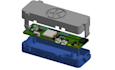
Collaborated with multiple teams at Oasis to engineer a highly durable, battery-powered industrial IoT device. Because the device was designed for remote deployments with minimal human interaction, mission-critical reliability was the top priority. I delivered an end-to-end solution, handling the custom hardware design, robust firmware development (including WiFi, OTA updates, and MQTT protocols),
Apr 2024
Mobile Outfitters
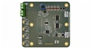
Partnered with Mobile Outfitters to engineer the core electronics for a high-precision, CNC-style mobile accessory cutting machine. Tasked with solving a complex integration of digital and analog circuits, I managed the full hardware lifecycle—from initial schematic design and high-density PCB layout to troubleshooting and prototype testing. The project resulted in a fully manufacturable, producti
Feb 2025-Feb 2026
What do you need to start?
Schematic or block diagram, component requirements, and board constraints (size, connector positions, layer count). A hand sketch is fine I will take it from there.
Do you support JLCPCB SMT assembly?
Yes. I deliver Gerber, BOM, and CPL files formatted specifically for JLCPCB or PCBWay assembly with no reformatting needed on your end.
Can you fix or audit an existing design?
Yes. Share your project files and I will identify layout issues, DRC violations, or DFM problems and fix them.
What is not included?
PCB manufacturing, component procurement, and firmware are not part of this gig. I offer firmware separately message me for a bundled quote.