Browse categories
Explore
Fiverr Pro
English
$
USD
Hardware and IoT Specialist
Level 2
Has met high performance criteria and has a proven track record for meeting client expectations.
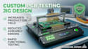
Get production-ready functional testing Jig for your PCBs
I provide professional PCB Testing Jig Design services to help you eliminate assembly errors and increase manufacturing yield. Whether you need a simple manual jig or a complex industrial "Bed of Nails" fixture, I deliver high-precision engineering files ready for fabrication.
What You Get:
️
Why This Service?
Please message me with your PCB Gerber or STEP files before ordering for a custom quote

Specialization:
Circuit design
•
Schematics
•
Layout
•
Footprint
File format:
Gerber
•
STEP
•
SCH
•
Software:
Altium Designer
•
EasyEDA
•
KiCad

Oasis Water Technologies
Collaborated with multiple teams at Oasis to engineer a highly durable, battery-powered industrial IoT device. Because the device was designed for remote deployments with minimal human interaction, mission-critical reliability was the top priority. I delivered an end-to-end solution, handling the custom hardware design, robust firmware development (including WiFi, OTA updates, and MQTT protocols),
Apr 2024

Mobile Outfitters
Partnered with Mobile Outfitters to engineer the core electronics for a high-precision, CNC-style mobile accessory cutting machine. Tasked with solving a complex integration of digital and analog circuits, I managed the full hardware lifecycle—from initial schematic design and high-density PCB layout to troubleshooting and prototype testing. The project resulted in a fully manufacturable, producti
Feb 2025-Feb 2026
What files do I need to provide to start the design?
To begin your custom PCB testing jig design, I need your PCB Gerber files (RS-274X or X2) or a 3D STEP file of your board. Please clearly mark the test points or pogo pin landing pads you need to probe for functional testing.
Do you provide the physical testing jig or just the design?
This gig is for the professional engineering design. You will receive all the necessary 3D CAD (STEP/STL) and 2D manufacturing files required to 3D print, CNC, or laser cut the fixture yourself, along with a complete BOM for pogo pins.
Can you design a "Bed of Nails" for double-sided PCBs?
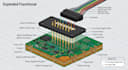
Yes. I specialize in both single-sided and complex double-sided pogo pin fixtures. For double-sided boards, I design a vertical alignment system that ensures high-precision contact for both top and bottom FCT (Functional Circuit Test) points.
Will I get a list of the exact pogo pins and hardware to buy?
Absolutely. Every order includes a detailed Bill of Materials (BOM). I provide specific part numbers and sourcing links (Digikey, Mouser, or LCSC) for the pogo pins, receptacles, and toggle clamps used in the design.
Is the design optimized for 3D printing or CNC machining?
I can optimize the test fixture enclosure for your preferred fabrication method. Just let me know if you plan to use FDM/SLA 3D printing or CNC milling (Acrylic/Delrin), and I will adjust the tolerances and wall thicknesses accordingly.


