Browse categories
Explore
Fiverr Pro
English
$
USD
Professional PCB Designer Precision and Reliability
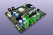
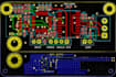
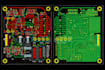
I will create professional PCB layouts from your schematics using Altium Designer, one of the industrys leading PCB development tools.
As a qualified Electronics Engineer with over 3 years of experience, I specialize in circuit development, embedded systems, schematic capture, and multi-layer board layout.
My expertise covers a wide range of applications, including:
With experience in Altium Designer, I ensure that every project is optimized for performance, manufacturability, and compliance with industry standards.
Deliverables include:
What software do you use for PCB design?
I use Altium Designer for all PCB layouts, schematics, and Gerber file generation.
Can you design multi-layer or high-speed PCBs?
Yes! I specialize in 2–4 layer PCBs for Industrial/IoT boards and complex high-speed/RF PCBs.
Can I contact you before placing an order?
Yes! I recommend contacting me for custom projects or questions to ensure your project requirements are fully understood.
What do you need from me to start the PCB design?
I need your schematic, circuit diagram, hand sketch, BOM, dimensions, and any special requirements for the PCB.
Do you provide manufacturing files?
Yes, I provide Gerber files, drill files, Pick and Place files, and other production-ready outputs.


