I will review and fix pcb design, schematic and layout issues

Germany

I speak English, German

Electronic engineer, pcb designer and firmware expert

Hi, I’m Hans Klünder, a professional electronics and PCB design engineer specializing in end to end hardware development solutions. I help individuals, startups, and businesses turn ideas into fully ...
About this Gig

Welcome to my Gig!

I help you review, debug, and optimize your PCB designs to ensure they are error free, reliable, and fully ready for manufacturing.


If you already have a schematic or PCB layout, I will carefully analyze it to identify design issues, improve circuit performance, and ensure your project meets proper engineering and fabrication standards.


My focus is on preventing costly mistakes before production by improving electrical performance, layout quality, and overall design reliability using professional PCB engineering practices.


What You Will Get

  • PCB schematic & layout review
  • Error detection report
  • Design improvement suggestions
  • Manufacturing readiness check
  • Performance optimization notes
  • Footprint & component verification
  • Signal integrity improvements
  • EMI reduction suggestions
  • Layout correction guide
  • Fabrication (DFM) feedback
  • Gerber file validation
  • Final engineering recommendations


Key Deliverables

  • Design issues report
  • Optimized PCB suggestions
  • Manufacturing-ready improvements
  • Clean, corrected layout guidelines
  • Performance upgrade notes


Message me before placing an order so we can review your PCB requirements and make sure you get the best possible optimization
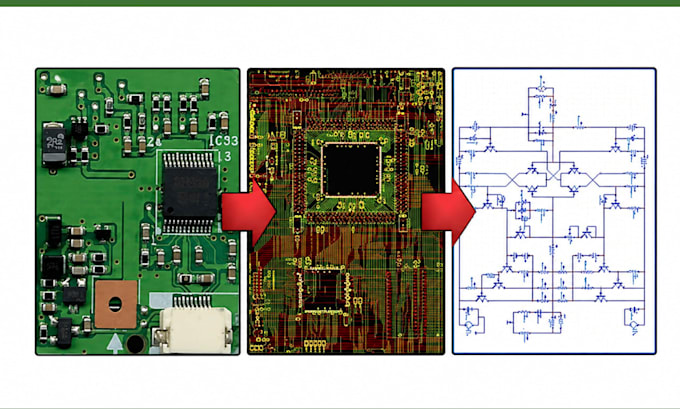
Specialization:

Circuit design

Schematics

Layout

Footprint

File format:

Gerber

BRD

SCH

PDF

ODB

Software:

Altium Designer

EasyEDA

Fusion 360

KiCad

AutoCAD

Interface:

HDMI

MIPI DSI/CSI

TDM

UART

USB

SPI

I2C

SDIO

PCIe

BLE

GSM/GPRS

Other Electronics Engineering Services I Offer