Browse categories
Explore
Fiverr Pro
English
$
USD
Hello and Welcome!
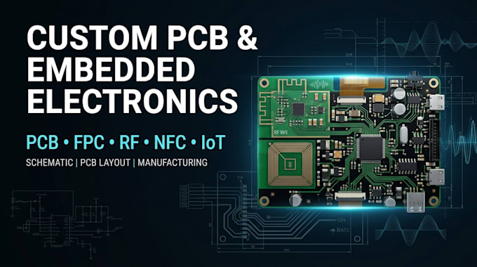
Modern electronic products are constrained by more than schematic correctness stack-up, impedance, RF return paths, antenna coupling, flex geometry, power integrity, thermal behavior, and manufacturability all have to work together.
I can translate your requirements into a practical hardware design.
What I Will Provide:
Why Choose Me
Have a schematic, prototype, reference board, datasheet, product idea, or only a technical concept? message now to get started!!
Can you design custom PCBs from scratch?
Yes. I can develop the schematic, component selection, PCB layout, and manufacturing files from your requirements.
Do you design flexible PCBs (FPC)?
Yes. I can design compact FPC solutions for wearables, sensors, connectors, and space-constrained electronics.
Can you handle RF and NFC designs?
Yes. I can work on RF/NFC circuits, antenna layouts, matching networks, grounding, and controlled-impedance routing.
What PCB software do you use?
I primarily work with professional PCB design tools such as KiCad, Altium Designer, and EasyEDA.
Can you design multilayer PCBs?
Yes. I can design 2-layer, 4-layer, 6-layer and more complex multilayer boards.