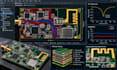
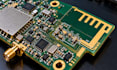
I will design rf pcb layout with antenna matching and impedance control

United Kingdom

I speak English, French, Spanish

Beyond the Possible!

Welcome to Hazeeln! I specialize in PCB design and electronics engineering, helping individuals, startups, and businesses turn their electronic concepts into practical, well-structured circuit board ...
About this Gig

WELCOME TO MY GIG!


Working on a WiFi, Bluetooth, LoRa, or wireless RF product? The PCB layout is critical to how your antenna and RF signals perform.


I design RF PCB layouts with antenna integration, controlled impedance routing, and RF signal-path planning, based on your circuit, operating frequency, and board specifications.


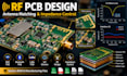
RF PCB DESIGN SERVICES


  • RF PCB layout and antenna integration
  • 50Ω controlled impedance routing
  • PCB antenna placement and feed-line routing
  • RF impedance matching network layout
  • Microstrip and coplanar waveguide routing
  • RF grounding and return-path planning
  • Multilayer RF PCB stack-up
  • WiFi, Bluetooth/BLE, LoRa and IoT PCB layouts
  • Gerber, BOM and fabrication files


WHAT I NEED FROM YOU


Your schematic, target frequency, antenna specifications, impedance requirements, board dimensions, layer count, and manufacturer constraints.


Whether you're developing a wireless IoT device, Bluetooth module, WiFi product, or custom RF circuit, let's discuss your design requirements before ordering.


Thanks!
Specialization:

Circuit design

•

Schematics

•

Layout

•

Simulations

File format:

Gerber

•

STEP

•

VRML

•

3DS

•

PDF

Software:

Allegro

•

Altium Designer

•

DipTrace

•

Fusion 360

•

KiCad

•

AutoCAD

Interface:

HDMI

•

MIPI DSI/CSI

•

I2S

•

TDM

•

UART

•

USB

•

SPI

•

I2C

•

SDIO

•

PCIe

•

Wi-Fi

•

BT