Browse categories
Explore
Fiverr Pro
English
$
USD
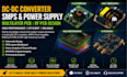
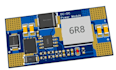
I'm an experienced electronics and PCB designer focus in DC-DC converters, SMPS, power supply circuits, multilayer PCBs, and RF PCB deslgn. I deliver high performance, reliable, and manufacturable PCB solutions designed to your project requirements.
what i offer
Perfect For:
Lets Get Started!
Send me your project details today, and lets create a custom DC-DC, SMPS, multilayer, or RF PCB deslgn that meets your exact requirements!
What information do you need to start my PCB design?
I need your schematic, component list, board size, layer count, and any special design requirements.
Can you design DC-DC converters and SMPS PCBs?
Yes! I specialize in DC-DC converters, SMPS, and high-efficiency power supply PCB design.
Do you handle multilayer and RF PCB design?
Absolutely. I design multilayer PCBs and RF circuits with optimized signal integrity and performance.
Can you optimize my PCB for manufacturability?
Yes! I ensure layouts are manufacturable, error-free, and optimized for real-world performance.
What file formats will I receive?
You’ll get Gerber files, PCB source files, and schematic PDFs ready for manufacturing.
How long does it take to deliver a PCB design?
Delivery depends on complexity: basic PCBs in 2–3 days, multilayer or RF designs in 5–7 days.


