Browse categories
Explore
Fiverr Pro
English
$
USD
pcb design and embedded system
HELLO BUYER!!!
WELCOME!
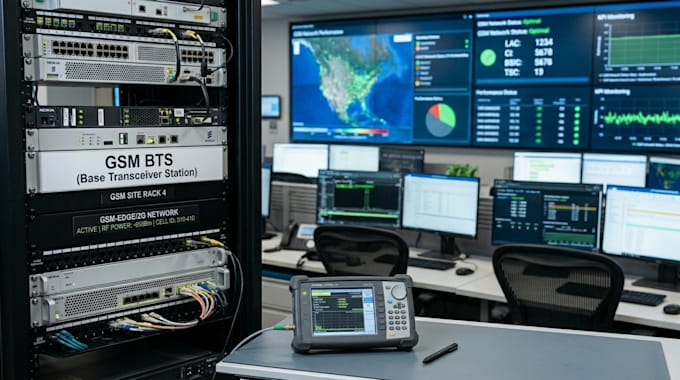
I specialize in designing high-quality RF and mixed signal PCBs optimized for signal integrity, electromagnetic compatibility, manufacturability, and reliable wireless performance. Whether you are developing an IoT device, GPS tracker, LoRa gateway, GSM communication module, industrial monitoring system, smart agriculture solution, or embedded wireless product, I can help transform your concept into a production ready PCB.
MY SERVICES INCLUDES;
WHY CHOOSE ME:
Contact me today with your project requirements, and let's create a reliable, high performance, and manufacturing ready wireless hardware solution tailored to your needs.


Which RF technologies do you support?
I work with GSM, GNSS, GPS, LoRa, LoRaWAN, LTE, WiFi, Bluetooth, BLE, Zigbee, and other wireless communication technologies.
Do you provide manufacturing ready files?
Yes. Deliverables include Gerber files, drill files, BOM, assembly documentation, and production ready outputs.
Can you optimize antenna placement and RF performance?
Absolutely. Proper antenna positioning, grounding, impedance control, and RF routing are key parts of my workflows