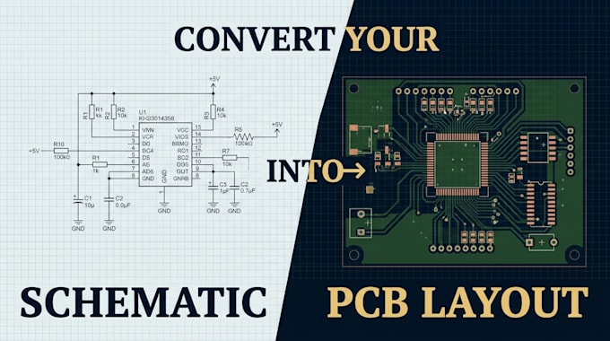
A bad layout can ruin a perfect circuit with signal noise, power drops, or assembly errors. I bridge the gap between your conceptual design and a physical, high-performing product. I specialize in converting raw schematics into industry-standard, manufacture-certified PCB layouts optimized for seamless fabrication.
What You Get with This Gig:
- DFM-Optimized Layouts: Every design strictly adheres to Design for Manufacturing (DFM) guidelines to eliminate assembly line delays.
- Signal & Power Integrity: I prioritize trace width calculations, controlled impedance, solid ground planes, and noise reduction for stable hardware performance.
- Multi-Layer Capabilities: Expert routing for complex 2-layer, 4-layer, or high-density multi-layer boards.
- Manufacturing Package: You receive complete industry-standard Gerber files (RS-274X/X2), Excellon drill files, and precise Pick-and-Place (CPL/BOM) coordinates optimized for automated assembly.
- Software Flexibility: Fully native project files delivered in Altium Designer, KiCad, or EasyEDA based on your workflow preference.
Perfect For: Custom IoT nodes, ESP32/Arduino shields, power supply modules, sensor arrays, and consumer eletronics.