Browse categories
Explore
Fiverr Pro
English
$
USD
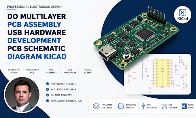
Trusted PCB Design Expert, From Schematic to Final Board
Expert Multilayer PCB De_sign & USB Hardware Development | Professional, Precise & Production-Ready
One error in your multilayer layout or USB trace routing can cost you weeks of rework and thousands in wasted production. I deliver professional, manufacturing-ready PCB designs & USB hardware solutions, circuit design, schematic diagram, PCB layout, using kicad, Altium designer, Arduino, Easyeda, Autocad, built to perform from first prototype to full production.
Here is what I offer:
Ready to get your PCB designed right the first time? Send me a message and let's talk about your project.


How many layers can you design?
I design PCBs from single layer up to 12 layers. The right layer count depends on your circuit complexity, signal routing requirements, and budget. I will always recommend the most cost-effective stack-up for your specific project before we begin.
Can you handle both the schematic and the PCB layout?
Yes. I cover the full design flow — from schematic capture and component selection through to PCB layout, DRC and ERC verification, and final manufacturing file generation. You receive a complete, production-ready package in one order.
What USB standards do you design for?
I design for USB 2.0, USB 3.0, and USB-C interfaces. Each design includes proper impedance controlled trace routing, ESD protection, power delivery circuitry, and signal integrity best practices specific to the USB standard being used.
Will my files be ready to send directly to a manufacturer?
Yes. Every completed design includes full Gerber files, drill files, BOM, and assembly files formatted and ready to upload directly to manufacturers like JLCPCB, PCBWay, or any manufacturer of your choice without any additional processing required.
Can you review and fix an existing PCB design?
Absolutely. I offer design review and optimization for existing PCB projects. Whether you need layout corrections, signal integrity improvements, or a full redesign, send me your project files and I will assess the scope before you place an order.