Browse categories
Explore
Fiverr Pro
English
$
USD
Need a reliable schematic or PCB design for an IoT or embedded electronics project? I will turn your requirements into a clear, manufacturable design using a practical engineering workflow.
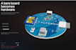
My experience includes connected sensor hardware such as Alteron Pulse, a compact environmental sensing device using an ESP32-C3, UART and I2C sensors, Wi-Fi connectivity, and a custom PCB.
Depending on your package, I can provide:
Circuit and schematic design
PCB layout for 2-layer or 4-layer boards
Component selection and bill of materials
Custom footprints
Gerber and fabrication files
Source files
STEP or 3D board model
Design-rule and manufacturability checks
I focus on readable schematics, sensible component placement, clean routing, and production-ready documentation. The final scope depends on board complexity, component count, interfaces, dimensions, and any special electrical or mechanical requirements.
Please contact me before ordering so I can review your requirements and recommend the right package. Component purchasing, physical manufacturing, assembly, firmware development, and certification are not included unless agreed separately.


File format:
Gerber
•
STEP
•
VRML
•
•
ODB
Software:
Fusion 360
•
Other
Interface:
I2S
•
UART
•
SPI
•
Wi-Fi
•
BLE
What information do you need before starting?
Please provide a functional description, preferred components, power requirements, interfaces, board dimensions, connectors, and any manufacturing constraints.
Does the service include PCB manufacturing or assembly?
The listed packages cover design files and documentation. Manufacturing, component purchasing, assembly, and shipping can be discussed as a separate custom project.
Can you also develop firmware for the PCB?
Firmware development is not included in the listed PCB packages, but I can review the requirements and provide a separate custom offer for embedded firmware.


