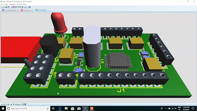
I provide professional PCB schematic design, layout, and optimization services for startups, hardware engineers, electronics hobbyists, and manufacturers worldwide. Whether you need a simple 2-layer board or a complex multi-layer PCB, I deliver precision-engineered designs that are ready for prototyping and mass production.
WHAT YOU GET:
- Complete PCB schematic capture and netlist generation
- Single, double, or multi-layer PCB layout design
- DRC (Design Rule Check) verified, zero-error files
- Gerber files, BOM (Bill of Materials), and drill files
- Design optimized for signal integrity and thermal management
- Impedance-controlled routing for high-speed designs
- Manufacturing-ready files (compatible with JLCPCB, PCBWay, OSH Park, and more)
- Support for single-layer, double-layer & multilayer PCBs
- Arduino, ESP32, STM32 & IoT-based circuit design
- Manufacturing-ready files for JLCPCB, PCBWay.
INDUSTRIES I SERVE:
- RF & Wireless Automotive
- Consumer Electronics
- Power Electronics
- IoT & Embedded Systems
- Electronics engineers
- Startups & hardware developers
- IoT and embedded system projects
- Arduino / ESP32 / STM32 projects
- Product prototyping and
CONTACT NOW AND LET GET STARTED !