Browse categories
Explore
Fiverr Pro
English
$
USD
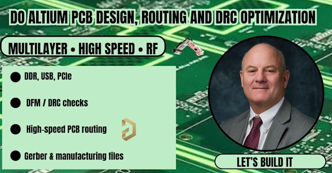
Are you looking for a professional Altium PCB specialist to turn your schematic into a clean, reliable, and manufacturing-ready board?
I provide professional Altium PCB layout, component placement, routing, and DRC optimization for electronic projects of different complexities.
Whether you need a new PCB layout, improvements to an existing board, or help preparing your project for manufacturing, I can help create a well-organized and properly optimized Altium project.
What I can provide:
Why work with me?
Attention to detail
Send me your schematic, PCB files, requirements, or project specifications, and let's get started.
File format:
Gerber
•
STEP
•
BRD
•
3DS
•
ODB
Software:
Allegro
•
Altium Designer
•
EasyEDA
•
Fusion 360
Interface:
MIPI DSI/CSI
•
I2S
•
USB
•
SPI
Can you work from a schematic only?
Yes. If you provide a complete schematic and the required component information, I can create the corresponding PCB layout in Altium.
Can you handle multilayer PCBs?
Yes, I can work with multilayer boards and handle layer stackups, routing, power planes, and signal integrity considerations.
: Can you work with an existing Altium PCB?
You can provide your schematic, Altium project files, PCB files, component list, datasheets, or any available project requirements.