Browse categories
Explore
Fiverr Pro
English
$
USD
Electronics Hardware Engineer
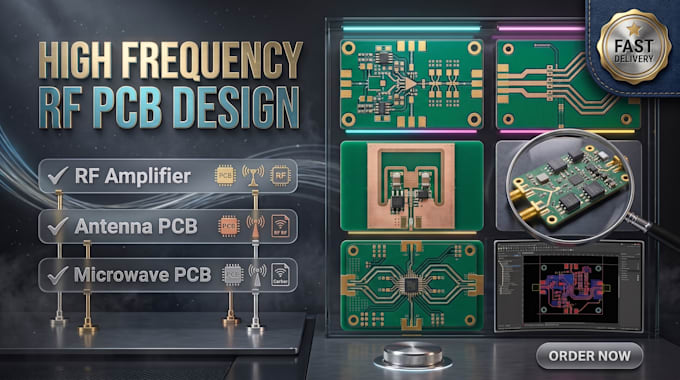
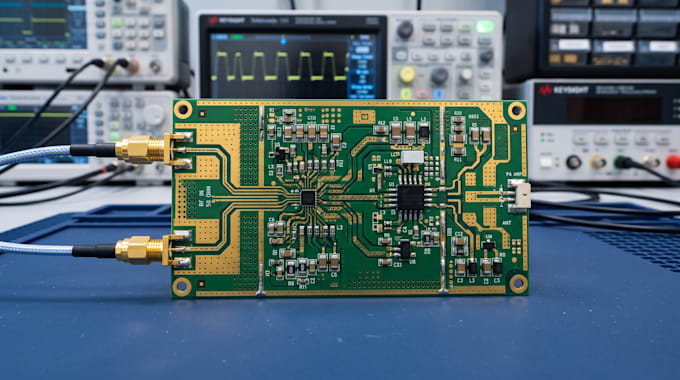
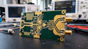
Designing a high frequency PCB requires more than placing components. A good RF PCB needs proper impedance control, controlled routing, low signal loss, and a layout that is ready for manufacturing.
I will design a professional high frequency PCB for RF amplifiers, antennas, microwave circuits, wireless communication, and other RF applications. Every design is created with performance, reliability, and manufacturability in mind.
What I Offer
Why Choose Me
Send your schematic, PCB requirements, or project details, and I'll provide the best solution for your RF PCB project.
What do you need to start the project?
I need your schematic, PCB requirements, dimensions, preferred PCB stack-up, and any design specifications.
Which PCB software do you use?
I work with industry-standard PCB design software based on your project requirements.
Will I receive manufacturing files?
Yes. You will receive production-ready Gerber files and other required manufacturing files.
Can you design impedance controlled PCBs?
Yes. I can design controlled impedance PCB layouts for high frequency applications.
Can you redesign or improve an existing PCB?
Yes. I can optimize and improve existing RF PCB layouts for better performance