Browse categories
Explore
Fiverr Pro
English
$
USD
Need a professional PCB design for your electronics project? I provide complete PCB design and PCB layout services for everything from simple prototypes to advanced multilayer boards used in complex electronic systems.
What I deliver
Whether you need a compact board for a small project or a complex multilayer PCB for advanced electronics, I ensure the layout is organized, properly routed, and ready for fabrication.
I work with makers, startups, and engineering teams who need reliable PCB designs completed accurately the first time with attention to signal integrity, manufacturability, and overall board quality.
Before ordering
Please send your project details, including:
Ill review the specifications and recommend the most suitable package for your project.
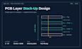
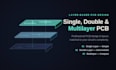
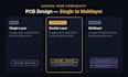
What's the difference between single, double, and multilayer PCB?
A single-layer PCB has one copper layer, best for simple circuits. A double-layer PCB has two copper layers, suited for intermediate complexity. A multilayer PCB has more than two layers, used for complex, high-density circuits with more components and connections.
Which package do I need for my project?
It depends on your circuit's complexity, component count, and board size. Message me your project details before ordering and I'll recommend the right tier, Single, Double, or Multilayer.
What files will I receive?
Fabrication-ready Gerber files, a Bill of Materials (BOM), and the PCB layout/schematic source files.
Do you handle component placement and routing?
Yes, full component placement and routing optimized for signal integrity and manufacturability are included in every package.
Can you design a PCB from my schematic, or do you also create the schematic?
Both. I can design from an existing schematic, or create the schematic from scratch based on your circuit requirements.
Will my design be ready for manufacturing?
Yes. Every design is checked for design rule compliance (DRC) before delivery, so your Gerber files are ready to send straight to a PCB manufacturer.


