Browse categories
Explore
Fiverr Pro
English
$
USD
An Expert RF PCB and PCB Antenna Design for Wireless Projects
WELCOME TO MY GIG
Hello I'm Casemiro F,
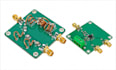
Are you struggling with poor RF performance, weak antenna range, signal loss, or unstable wireless connectivity in your IoT product? I work on professional RF PCB and PCB antenna optimized for WiFi, BLE, GSM, GPS, LoRa, and other high frequency wireless applications.
This gig is ideal for IoT startups, embedded engineers, smart device developers, ESP32 projects, wireless sensor systems, and custom electronics products.
what you will get:
software used:
Deliverables:
kindly send me your project ideas now and lets build a reliable RF PCB for your wireless device. Every design is optimized for signal integrity, RF stability, compact routing, and smooth PCB manufacturing to reduce costly prototype errors. looking forward to work with you and serves you the best designs that'll leave your competitors speechless !!!

What do you need to start my RF PCB or PCB antenna project?
Please provide your schematic, dimensions, preferred RF module, frequency range, antenna type, and design requirements. If you only have an idea, I can still help you develop a manufacturable RF PCB layout.
Can you design RF PCBs for WiFi, BLE, GSM, GPS, and LoRa devices?
Yes. I design high frequency RF PCB layouts and PCB antennas for WiFi, Bluetooth, BLE, GSM, GPS, LoRa, ESP32, nRF52, and other IoT wireless devices with controlled impedance and optimized RF routing.
Which software do you use for RF PCB design?
I use Altium Designer, KiCad, and EasyEDA for professional RF PCB layout, antenna integration, impedance routing, and production-ready PCB manufacturing files.
What files will I receive after project completion?
You will receive Gerber files, source files, BOM, pick and place files, PDFs, fabrication files, and other manufacturing deliverables required for PCB production and assembly.
Can you help improve weak antenna range or RF performance issues?
Yes. I can optimize antenna placement, grounding, RF routing, impedance matching, and EMI performance to help reduce signal loss, improve wireless stability, and increase antenna efficiency in IoT devices.


