Browse categories
Explore
Fiverr Pro
English
$
USD
Expert Electrical Engineer for PCB Design and IoT Solutions
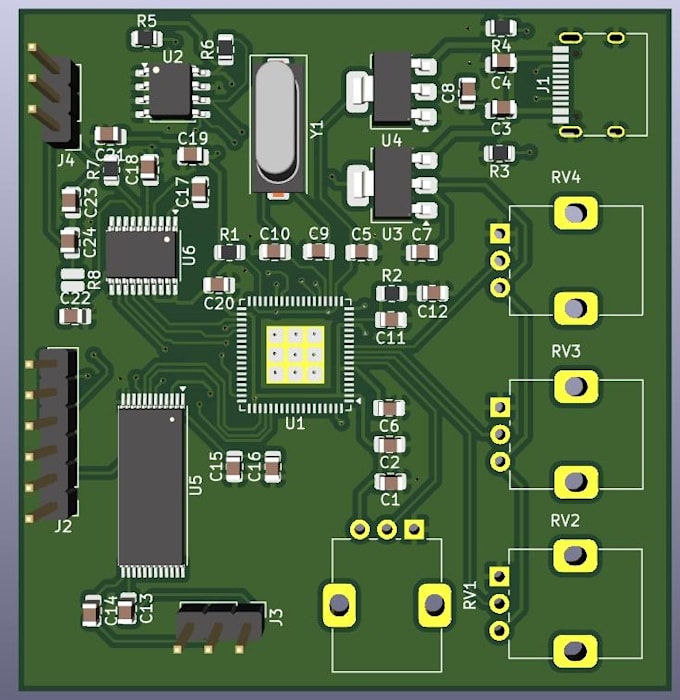
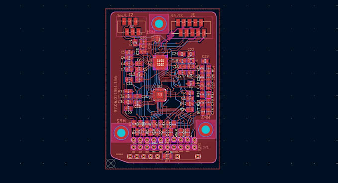
I am an Electrical Engineer with specialized expertise in high-performance PCB design and IoT solutions. Using KiCad,EasyEDA. I can transform your schematic ideas into a manufacturing-ready hardware reality. From simple breakout boards to complex high-speed multi-layer PCBs, I focus on signal integrity, compact layout, and thermal management.
I will provide you with the following files:
I dont just route traces; I ensure your hardware is stable, noise-free, and ready for mass production. Lets collaborate to build reliable and professional electronics!


File format:
Gerber
•
STEP
•
SCH
•
3DS
•
Software:
EasyEDA
•
KiCad
•
Proteus
•
AutoCAD
•
CST Studio Suite
•
Arduino
Interface:
I2S
•
UART
•
USB
•
SPI
•
I2C
•
Wi-Fi
•
BLE
•
GSM/GPRS
•
NB-IoT
Which software do you use for PCB design?
I use KiCad and EasyEDA for all my professional PCB design projects, ensuring high-quality industry-standard output files.
Can you help with component selection and sourcing?
Yes! I can select cost-effective and available components from distributors and provide a complete BOM.
Do you design multi-layer PCBs and high-speed circuits?
Absolutely. I have experience in 4-layer and 6-layer designs, including high-speed signal routing and impedance control.