I will create rf pcb design for iot, GSM, gps and wireless devices

United Kingdom

I speak English

PCB Layout Design

I am a professional PCB Layout Designer and Electronics Hardware Developer with strong experience in transforming circuit concepts into high-performance, manufacturable PCB designs. I specialize in de...
About this Gig

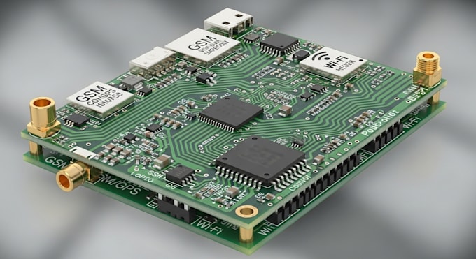
I will create high-performance RF PCB designs for IoT, GSM, GPS, and wireless devices engineered for precision, stability, and real-world signal performance. Designing RF boards is not just routing traces it requires controlled impedance, noise suppression, and careful RF path optimization. I deliver production-ready PCB designs that ensure strong connectivity, minimal interference, and maximum efficiency. From IoT smart devices to GSM/GPS trackers, BLE, WiFi, and LoRa systems, I help turn your concept into a robust, manufacturable RF product


What Youll Get

  • RF Schematic Design & Optimization
  • Multi-layer PCB Layout (212 Layers)
  • Controlled Impedance Routing (50Ω RF lines)
  • Antenna Matching & RF Tuning Support
  • EMI/EMC Noise Reduction Techniques
  • Signal Integrity Optimization
  • Gerber, BOM, Pick & Place Files
  • DFM & DFA for Manufacturing


Why Choose Me?

  • Specialized in RF & Wireless PCB Design
  • Focus on performance, not just connections
  • Clean, optimized & production-ready files
  • Fast delivery & professional communication


Contact me now to get a reliable, high-performance RF PCB design ready for manufacturing and real-world deployment.

Specialization:

Circuit design

Schematics

Layout

Footprint

File format:

Gerber

STEP

VRML

BRD

PDF

Software:

Allegro

Altium Designer

Cadence OrCAD

Eagle CAD

EasyEDA

Interface:

HDMI

MIPI DSI/CSI

I2S

UART

USB

SPI

I2C

Wi-Fi

BLE

BT

GSM/GPRS