I will design custom multiplayer pcb with schematic, bom, kicad and gerbers files

United States

I speak English

PCB Design

I'm experienced PCB Design Engineer and Electronics Developer specializing in high-quality schematic design, PCB layout, and manufacturing-ready board development for prototypes and production. With s...
About this Gig

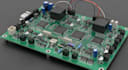
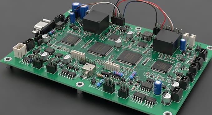
Get a professional custom multilayer PCB design complete with schematic, BOM, KiCad files, and manufacturing-ready Gerber files. This service is ideal for prototypes, embedded systems, IoT devices, and commercial electronic products. Your PCB will be carefully designed with optimized component placement, clean routing, and proper design rules to ensure reliability and smooth manufacturing. I focus on creating high-quality, production-ready designs that meet industry standards.


What This Service Includes

  • Custom multilayer PCB de sign (2, 4, 6+ layers)
  • Professional schematic circuit design
  • Optimized component placement and PCB routing
  • Detailed Bill of Materials (BOM) with components list
  • KiCad source project files for easy editing
  • Gerber manufacturing files ready for PCB fabrication
  • Create optimized for PCB manufacturers such as JLCPCB, PCBWay, and others
  • Create rule checks (DRC) and verification before delivery


Why Choose This Service

  1. Professional PCB designer with strong electronics expertise
  2. Clean, optimized layouts for performance and reliability
  3. Manufacturing-ready deliverables
  4. Clear communication and dedicated project support
  5. High-quality De sign


ORDER NOW!!

Specialization:

Circuit design

Schematics

Layout

Footprint

File format:

Gerber

STEP

VRML

BRD

SCH

Software:

Altium Designer

Cadence OrCAD

DipTrace

Eagle CAD

EasyEDA

Interface:

HDMI

MIPI DSI/CSI

I2S

TDM

UART

USB

SPI

I2C

SDIO

PCIe

Wi-Fi

BLE

Related tags