I will create iot devices and smart products with multi layer pcb and kicad schematic

United States

I speak English

PCB Layout design

I am a skilled PCB designer and electronics developer dedicated to helping startups, engineers, and innovators build reliable circuit boards for their projects. From schematic design to final producti...
About this Gig

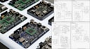
Delivering well-functioning IoT devices and smart products with multi-layer PCB layouts and professional KiCad schematics. Every design is engineered for reliability, manufacturability, and real-world performance, ensuring your hardware works flawlessly in industrial, commercial, or prototype applications.


Services Offered

  1. Custom multi-layer PCB design for ESP32 or embedded systems
  2. KiCad schematic creation with full production readiness
  3. IoT hardware integration including sensors, modules, and connectivity
  4. Component selection & circuit optimization for efficiency and stability
  5. Complete manufacturing files: Gerber, BOM, and fabrication-ready layouts


Why Choose This Service

  1. Professional, production-ready PCB and schematic design
  2. Optimized for performance, signal integrity, and manufacturability
  3. Full project support from concept to production
  4. Designed for serious IoT
  5. Embedded system projects


Bring your IoT project to life with a professional multi-layer PCB and smart product design. Send your project requirements today, and lets build your IoT device!

Specialization:

Circuit design

Schematics

Layout

Footprint

File format:

Gerber

STEP

VRML

BRD

SCH

Software:

Altium Designer

Cadence OrCAD

Eagle CAD

EasyEDA

KiCad

Interface:

HDMI

MIPI DSI/CSI

I2S

TDM

UART

USB

SPI

I2C

SDIO

PCIe

Wi-Fi

BT