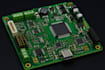
I will create a custom PCB schematic, component placement, PCB layout, routing, and Gerber files based on your project requirements. Whether you are developing a prototype, IoT device, embedded system, controller, sensor board, or custom electronics product, I will focus on creating a clean and functional PCB design.
What I Can Provide
- Custom PCB schematic design
- Professional PCB layout
- Component placement and footprint selection
- PCB routing and trace optimization
- 2-layer and multilayer PCB design
- Design rule checking (DRC)
- Electrical rule checking (ERC)
- Ground planes and power routing
- Connector and component integration
- Board outline and mounting holes
- Design for manufacturing considerations
- Gerber and drill files
- BOM (Bill of Materials), when required
- Source/project files
- Manufacturing-ready PCB files
Why Choose My Service?
- Clean and professional PCB layouts
- Attention to component placement and routing
- Manufacturing-ready output files
- Organized project/source files
- Design checks before delivery
- Clear communication throughout the project
- Suitable for prototypes and product development
- Custom solutions based on your requirements
Please contact me before placing an order