Browse categories
Explore
Fiverr Pro
English
$
USD
PCB Designer, RF, Rigid Flex, Wearable, IoT, Multilayer PCB Schematic, Jlcpcb
Are you looking for a professional PCB designer who can deliver high quality schematic, RF, multilayer, rigid flex, and wearable IoT circuit board designs that are ready for manufacturing?
I'm a PCB design engineer with extensive experience in advanced electronics hardware development. I focus on creating clean, efficient, and manufacturable PCB layouts for startups, engineers, and product developers who demand excellence.
What I Deliver:
Every deslgn prioritizes signal integrity, EMI/EMC compliance, power efficiency, thermal management, and Design for Manufacturability (DFM) ensuring smooth production and first time right boards in 2026s demanding market.
Lets bring your hardware project to life with confidence. Message now and let's get started.
What types of PCB designs do you specialize in?
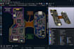
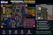
I specialize in advanced PCB schematic design, high-frequency RF PCB, multilayer boards, rigid-flex, flexible, wearable, and IoT PCB layouts. I regularly work on ESP32, SoC FPGA, high speed digital, and antenna designs, all optimized for JLCPCB and PCBWay manufacturing and assembly.
Are your PCB designs ready for manufacturing?
Yes. Every design is delivered 100% production ready. You will receive complete Gerber files, BOM, CPL (Pick & Place), 3D STEP model, assembly drawings, and full DFM (Design for Manufacturability) checks to ensure smooth fabrication and assembly at JLCPCB or PCBWay.
How experienced are you with RF and Rigid Flex designs?
I am a premium PCB designer with strong expertise in high frequency RF PCB design, impedance control, antenna integration, and complex rigid-flex projects. These are among my most requested services for wearable, medical, and industrial IoT applications.
What information do I need to provide to start a project?
Please send your schematic (even if hand-drawn), block diagram, requirements, size constraints, key components, and any specific standards (RF performance, power, etc.). The clearer the brief, the faster and better the final result.
Do you provide support after delivery?
Yes. Premium clients receive ongoing technical support. I stand behind my work and will assist with any manufacturing issues or minor adjustments needed at the fabrication stage.
Why should I choose you over cheaper PCB designers?
I deliver premium, first-time-right designs with professional documentation that fabricators love. My focus is on signal integrity, EMI reduction, power efficiency, and DFM, which saves clients time and money on failed prototypes and re-spins.


