Browse categories
Explore
Fiverr Pro
English
$
USD
PCB Designer, RF, Rigid Flex, Wearable, IoT, Multilayer PCB Schematic, Jlcpcb
Looking for a professional PCB schematic and layout design that is reliable, manufacturable, and ready for production? I deliver high quality PCB solutions for IoT devices, robotics, consumer electronics, and industrial applications.
As a specialized PCB design engineer, I help hardware developers, startups, and engineers create clean, efficient, and production ready boards using modern design practices.
What I Offer:
Every design focuses on Design for Manufacturability (DFM), signal integrity, power integrity, thermal management, and EMI reduction ensuring smooth production and high reliability in 2026s competitive market.
Lets build reliable and professional electronics together.
What types of PCB designs do you specialize in?
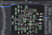
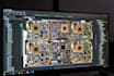
I specialize in professional PCB schematic capture and layout design for rigid, flexible, rigid-flex, and high-layer count multilayer boards (up to 12+ layers). My expertise covers IoT devices, robotics, consumer electronics, and complex high-speed designs.
Do you provide complete files ready for JLCPCB assembly?
Yes. Every package includes full Gerber files (RS-274X), drill files, optimized BOM (with LCSC/JLCPCB part numbers and alternatives), and accurate CPL (Pick & Place) files. I also provide assembly drawings, 3D STEP models (in higher packages), and a comprehensive DFM report
Which PCB design software do you use?
I am highly proficient in Altium Designer, KiCad, and EasyEDA. I deliver native source files along with all manufacturing outputs. Most clients prefer Altium for complex projects due to its superior capabilities in multilayer, high-speed, and rigid-flex designs.
How fast can you complete my PCB design project?
Delivery time depends on complexity
Can you handle high-speed, impedance control, and IoT/robotics designs?
Absolutely. I regularly design high-speed digital, RF, and mixed-signal boards with impedance control, length matching, differential pairs, and proper power integrity considerations. My designs are optimized for signal integrity, thermal management, and EMC performance
What do I need to provide to start my project?
To deliver the best results, please provide: Schematic (hand-drawn or partial is fine) Requirements (size constraints, features, interfaces, etc.) Preferred stack-up and layer count Any mechanical constraints or enclosure dimensions Special requirements (high current, RF, impedance, etc.)
Why should I choose your premium PCB design service?
I focus on delivering production-ready designs that minimize manufacturing risks, reduce assembly costs, and eliminate expensive respins. My clients choose me for professional DFM/DFA optimization, clear documentation, responsive communication, and designs that go straight to successful JLCPCB


