Browse categories
Explore
Fiverr Pro
English
$
USD
Professional PCB Designer, Altium KiCad EasyEDA, IoT ESP32 STM32 RF High Speed
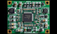
I will design production ready IoT PCB for ESP32 STM32 Gerber BOM CPL DFM expert
Launch your smart device with confidence. As a top rated hardware engineer with 8+ years specializing in IoT PCB design, I deliver ESP32 and STM32 layouts that pass first-time manufacturing at JLCPCB, PCBWay & Seeed no costly respins.
You get clean, DFM-optimized boards ready for 10010,000 unit runs, incorporating 2026 trends: Wi-Fi 6 / Thread / Matter support on ESP32-C6/S3, Edge AI acceleration, ultra low power STM32H5 layouts, impedance controlled 4-layer stacks, RF antenna matching, and signal integrity for reliable BLE / Zigbee / LoRa connectivity.
What you receive:
Choose Basic for quick prototypes, Standard for production launch, or Premium for full embedded systems + RF tuning + unlimited revisions.
Message me your requirements let's build a bulletproof board that wins certifications.

Do you design IoT PCBs with ESP32 or STM32?
Yes, I specialize exclusively in ESP32 and STM32-based IoT PCB design (including ESP32-S3/C6, STM32H5/H7 series). I create production-ready multilayer layouts optimized for Wi-Fi 6, BLE 5.x, Thread/Matter, LoRa, low-power Edge AI, and mixed-signal sensor integration all with proper RF matching.
Are the Gerber files, BOM, CPL, and DFM really manufacturing-ready?
Absolutely. Every package delivers complete, verified Gerber RS-274X files (all layers + drill + netlist), LCSC/JLCPCB-optimized BOM with alternates & cost-down suggestions, full CPL / pick-and-place + centroid files, detailed DFM / DFA report, 3D STEP model, and assembly drawings.
What information do I need to provide before ordering?
To deliver the best IoT PCB layout, please share: Functional block diagram or detailed requirements Preferred microcontroller (ESP32 / STM32 model) Key interfaces / peripherals / power budget Target size constraints & layer count Any existing schematic (even rough) or reference design
Can you fix or improve my existing ESP32 / STM32 PCB that failed manufacturing or has issues?
Yes, this is one of my most requested services. I perform full design reviews, fix DFM violations, optimize RF performance, improve EMI/EMC resilience, correct power distribution, and update files for reliable production. Send me your current Gerbers / schematic / photos of failed boards
Do you provide firmware or only hardware / PCB design?
The core service focuses on professional PCB design, schematic optimization, Gerber files, BOM, CPL, and DFM. Premium package includes basic bootloader, peripheral initialization, and FreeRTOS skeleton code.
Will my board pass certification (CE / FCC / etc.) on the first try?
While no designer can legally guarantee certification, my layouts follow 2026 best practices for EMI/EMC: proper grounding, decoupling, shielding, RF antenna clearance, and separation of noisy/digital sections. 90%+ of my clients pass pre-compliance testing with minimal tweaks.
Why choose your service over cheaper PCB design gigs?
You invest in prevention, not respins. Low-cost gigs often deliver error-prone layouts that cost $2,000–$15,000+ in failed prototypes, delayed launches, and lost funding. With 8+ years, 150+ manufactured boards, and consistent 5.0 feedback from IoT startups & scale-ups
