Browse categories
Explore
Fiverr Pro
English
$
USD
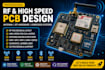
Are you looking for a professional RF and high speed PCB design engineer for your wireless project?
You are in the right place!
I will design high quality, industry standard PCB for:
Technologies I Work With:
What You Will Get:
Why Choose Me?
Contact me before placing an order to discuss your project.

What do you need to start my PCB design?
I need your circuit idea, sketch, or schematic. You can also send reference images, PDFs, or clear instructions about your project.
Can you convert my schematic into a PCB layout?
Yes, I can convert your schematic into a clean and professional PCB layout ready for manufacturing.
Will I get files ready for PCB manufacturing?
Yes, you will receive Gerber files and all required files that can be sent directly to any PCB manufacturer.


