Browse categories
Explore
Fiverr Pro
English
$
USD
Professional PCB Design Engineer Altium and KiCad Expert
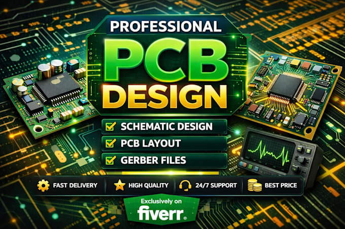
I will design professional ESP32 & IoT PCBs ready for production! From full schematic and PCB layout to Gerber files, BOM, pick-and-place files, and 3D renders, I deliver manufacturing-ready designs for microcontroller-based devices, sensors, and wireless modules. I specialize in 2-to-6-layer multilayer PCB layouts, optimized routing, EMI-safe designs, and high-speed signal integrity. Perfect for prototypes, IoT projects, and embedded systems, my work is precise, reliable, and on time. Whether you need a starter, advanced, or professional PCB, I ensure your design is production ready and easy to manufacture. Let's turn your hardware idea into reality message me now to get started!

What do you need from me to start the PCB design?
I need your project idea, schematic (if available), components list, and any special requirements. If you don’t have a schematic, I can create it from scratch.
Which software do you use for PCB design?
I use Altium Designer, KiCad, and EasyEDA, depending on your preference. All deliverables are compatible with standard PCB manufacturers.
Will the PCB be ready for manufacturing?
Absolutely! You will receive Gerber files, BOM, pick-and-place files, and 3D renders, all checked and production-ready for manufacturers like JLCPCB or PCBWay
Can you design multilayer or high-speed PCBs?
Yes! I specialize in 2–6 layer PCBs, high-speed circuits, EMI-safe designs, and optimized routing for IoT and embedded projects.
Do you offer revisions?
Yes! Each package includes 1–3 revisions depending on the package level. I ensure your PCB meets your specifications before final delivery.
Can you handle complex IoT or embedded projects?
Absolutely! I design microcontroller-based IoT devices, wireless modules, sensor circuits, and embedded systems from prototype to production-ready PCB.