Browse categories
Explore
Fiverr Pro
English
$
USD
PCB DESIGN AND FIRMWARE DEVELOPMENT
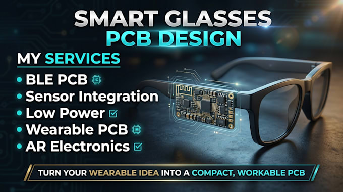
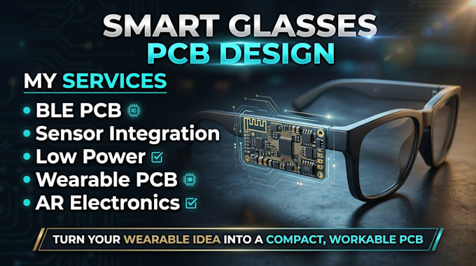
A smart wearable can fail long before the first prototype because the PCB is too large, drains the battery, loses BLE reliability, or cannot fit the sensors where they need to go. I help turn those constraints into a compact, practical PCB for AR glasses and other low-power wearables.
What You Will Get
What Makes Me Stand Out
I focus on the problems that matter after the schematic: space, power, signal integrity, component placement, and real world manufacturability not just making a board look complete.
Deliverables
Schematic, PCB layout, Gerber files, drill files, BOM, and relevant manufacturing documentation.
Have a wearable concept or an existing PCB that needs improvement? Send me your requirements and lets turn the constraints into a workable board.



Specialization:
Circuit design
•
Schematics
•
Layout
•
Footprint
•
Gerber
File format:
Gerber
•
STEP
•
BRD
•
SCH
•
Interface:
I2S
•
TDM
•
UART
•
USB
•
SPI
•
I2C
•
SDIO
•
PCIe
•
BLE
•
BT
•
NB-IoT
Can you make the PCB fit a small smart-glasses or wearable enclosure?
Yes. I can optimize component placement and board dimensions around your available space, sensors, battery, and enclosure requirements.
Can you integrate BLE, sensors, and low-power features?
Yes. I can incorporate BLE connectivity, sensors, power-management circuitry, and battery-conscious architecture based on your requirements.
What do you need from me before starting?
Ideally, send your requirements, available dimensions, preferred components, battery details, sensor list, and any existing schematic or reference files. If you’re still at the concept stage, I can work from your specifications.