Browse categories
Explore
Fiverr Pro
English
$
USD
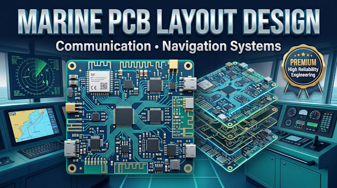
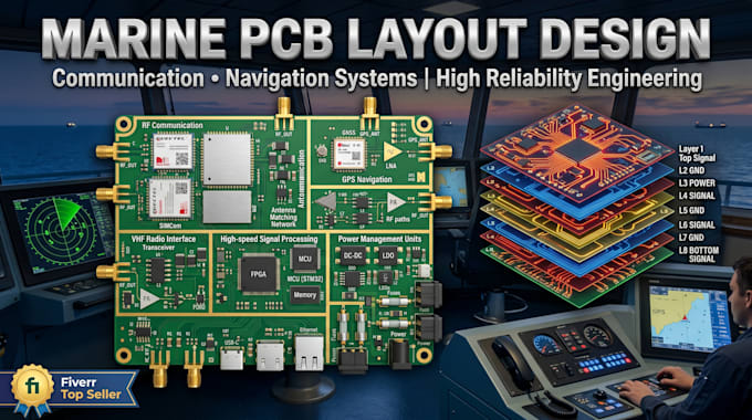
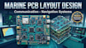
I can help turn your circuit idea, schematic, or concept into a clean, reliable, production-ready PCB layout built for marine and offshore electronic applications. From communication boards to navigation control systems, the goal is always the same a design that performs well, is easy to manufacture, and is built with quality in mind.
I can work on projects involving:
Whether you're building a navigation board, communication module, monitoring device, control interface, or marine electronic system, Ill make sure the PCB layout is properly arranged, professionally routed, and ready for production.
Clear communication, attention to detail, and quality work are what you can expect.
Send me a message with your project details before ordering.
Specialization:
Circuit design
•
Schematics
•
Layout
•
Analysis
File format:
Software:
Eagle CAD
•
EasyEDA
•
Fusion 360
•
AutoCAD
•
SolidWorks
Interface:
HDMI
•
I2S
•
UART
•
USB
•
Wi-Fi
•
BLE
•
LTE
•
NB-IoT
What do you need to start my PCB design project?
I need your schematic, project requirements, dimensions, and any preferred components if available.
Can you create the PCB layout from my circuit diagram?
Yes, I can turn your schematic or circuit concept into a complete PCB layout ready for manufacturing.
Do you provide 3D PCB design files?
Yes, I can provide realistic 3D PCB views along with the design files.
Which PCB design software do you use?
I work with industry-standard tools like Altium Designer, KiCad, and other professional PCB software when needed.
Can you design multilayer PCBs?
Yes, I can design single-layer, double-layer, and multilayer PCB layouts depending on your project needs.
Will I receive manufacturing files?
Yes, you will receive Gerber files, BOM, and all necessary production files for fabrication.
Can you redesign or modify an existing PCB?
Yes, I can update, resize, optimize, or redesign an existing PCB layout.
Do you handle marine communication and navigation systems?
Yes, I design PCB layouts for marine electronics, communication modules, navigation boards, and control systems.
How long does delivery take?
Delivery time depends on project complexity, but smaller designs are usually completed quickly.
Should I contact you before placing an order?
Yes, sending your project details first helps confirm the best package and delivery time.