Browse categories
English
$
USD
Connect to your AI
i create PCB layout for your electronic project?
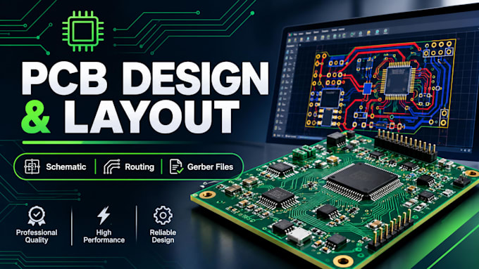
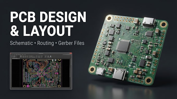
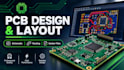
I provide accurate printed circuit board development, including schematic capture, component placement, copper routing and multilayer board development. Whether you need a simple 2-layer board or a complex electronic assembly, I focus on clean connections, proper spacing and manufacturing requirements.
MY SERVICES INCLUDE:
DELIVERABLES:
You can receive Gerber files, drill files, editable project files, BOM and PDF documentation, depending on your selected package.
I work with KiCad, EasyEDA and Altium Designer to produce organized, professional PCB layouts.
Send me your schematic, project requirements or reference files before ordering. Let's turn your electronic concept into a reliable, manufacturing-ready circuit board.
What information do you need to start a PCB design?
I typically need your circuit schematic, project requirements, component list and preferred board dimensions. If you have an existing design, you can also share the project files.
Can you design a PCB from scratch?
Yes. I can assist with schematic capture and PCB layout based on your functional requirements, component specifications and design goals.
Do you design multilayer PCBs?
Yes. I can work on single-sided, double-sided and multilayer PCB designs, depending on the project complexity.
Will I receive Gerber files for manufacturing?
Yes. Manufacturing deliverables can include Gerber files, NC drill files and other required production documentation.
Which PCB design software do you use?
I work with KiCad, EasyEDA and Altium Designer, depending on the project requirements and preferred file format.
Can you modify or repair an existing PCB layout?
Yes. I can help with layout modifications, component repositioning, routing improvements and design rule corrections.
Do you provide editable source files?
Yes. Editable project files are included according to the selected package.
Can you design a PCB according to my manufacturer's specifications?
Yes. Please provide your manufacturer's design rules, board dimensions, layer requirements and fabrication specifications before ordering.
Do you guarantee that the PCB will work perfectly after manufacturing?
PCB design checks help identify layout and connectivity issues, but they do not replace physical prototyping, electrical testing or functional validation.
Can I request a custom PCB design?
Absolutely. Contact me with your project details, complexity, preferred software and required deliverables for a tailored offer.