Browse categories
Explore
Fiverr Pro
English
$
USD
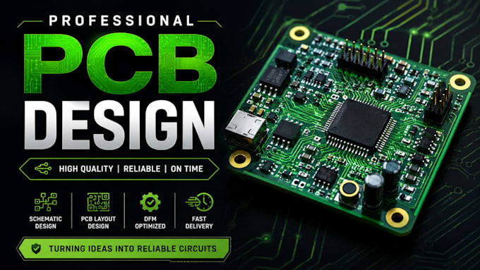
PCB Design and Schematic Expert, IoT and Circuit Solutions
Tired of ESP32 boards that work on breadboard but fail after fabrication? I'm Jan Lemann I design IoT PCBs that survive real-world deployment, not just bench demos.
Your IoT product deserves more than a dev kit crammed into a 3D printed box. I specialize in ESP32 and STM32 multi layer PCB design with WiFi/BLE RF routing, sensor integration, and power optimized layouts.
What you get:
My Process:
Why Choose Me:
Your competitors are already shipping. Contact me now with your sensor list and power requirements I'll reply with a block diagram and layer stackup recommendation within 12 hours. Let's get your IoT product out of prototype hell and into production.
CONTACT ME NOW!!!!
Which ESP32 or STM32 variant should I use?
I work with ESP32-WROOM, WROVER, C3, S3, C6, and STM32F1/F4/F7/H7 series. During our requirements call, I'll recommend the optimal MCU based on your WiFi/BLE needs, GPIO count, power budget, and cost target — then optimize antenna placement and memory routing for that specific variant.
I only have a rough idea and no schematic. Can you still help?
Absolutely. Most of my clients start with just a sensor list and a napkin sketch. I'll design the complete schematic from scratch, select components with available stock, and build the PCB layout — you don't need any prior design files.
How do you ensure my board will work after fabrication?
Three layers of protection: (1) ERC/DRC clean schematics and layouts before export, (2) JLCPCB/PCBWay DRC validation to catch fab-specific issues, (3) power integrity and signal integrity review for critical nets. My 95% first-pass success rate comes from designing for manufacturability, not just c
Can you design for battery-powered IoT with deep sleep?
es — this is my specialty. I optimize power paths, select the right LDO vs. buck converter, calculate sleep current budgets, and target <100µA deep sleep where your application allows. You'll receive a power consumption spreadsheet with estimated battery life before fabrication.
Do I own the design files, or are they locked to you?
You own everything. Premium includes full source files (.kicad_pcb, .sch, libraries). Even Basic/Standard packages include Gerber and manufacturing files you can take to any fabricator. No vendor lock-in, no hidden dependencies — your IP stays yours.
