Browse categories
Explore
Fiverr Pro
English
$
USD
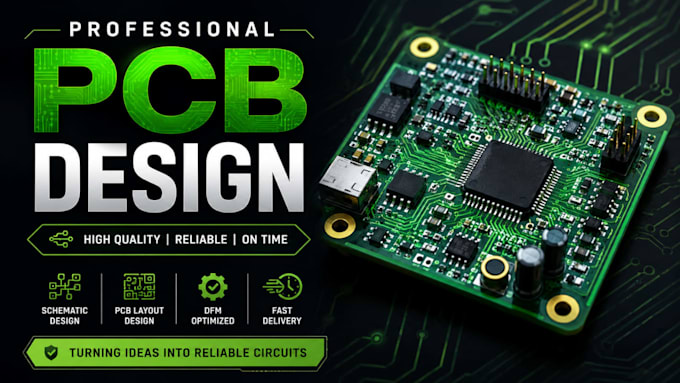
PCB Design and Schematic Expert, IoT and Circuit Solutions
From Sketch to Shipped Board, Without the Headaches
Every failed prototype costs time, money, and market momentum. I eliminate that risk by designing PCB layouts and circuit schematics that pass DRC/ERC on the first attempt then manufacturing validation on the first fabrication run.
When your PCB design involves DDR4 routing, BGA fanouts, or RF front ends, "good enough" isn't an option. I architect circuit boards that meet electrical, thermal, and mechanical constraints then document every decision so your team can maintain and scale the design.
Technical Deliverables:
Tools:
Let's build something real. Hit "Contact Seller" and tell me about your project I'll reply with a clear plan and honest timeline within a
What do you need from me to start?
Your schematic (or block diagram), target board size, connector requirements, and any critical component preferences. If you only have a concept, I can design the schematic from scratch.
Which PCB design software do you use?
KiCad is my primary tool for this gig. I also work in Altium, Eagle, and OrCAD if you need file format compatibility with your existing workflow.
What files will I receive?
Gerber RS-274X, NC drill, BOM with supplier part numbers, pick-and-place (CPL), 3D STEP model, PDF schematic, and PCB fabrication notes.
Can you design for JLCPCB / PCBWay assembly?
Yes. I validate all designs against JLCPCB and PCBWay DRCs and include their preferred BOM/CPL formats for seamless ordering.
Do you handle high-speed or RF PCB design?
Absolutely. I have experience with controlled impedance, DDR routing, USB 3.0+, and RF layouts up to 6GHz. Select the Premium package for complex designs.
