Browse categories
Explore
Fiverr Pro
English
$
USD
PCB Design Engineer, Automotive ECU, RF, HighSpeed and Power Electronics
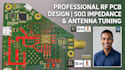
Need an expert to design high-frequency wireless hardware without signal degradation, cross-talk, or EMI failures? I specialize in professional RF PCB layout to ensure pristine signal integrity from schematic to factory.
Whether you are building a smart IoT node, a custom antenna network, or a complex microwave module, I structure every board with strict controlled impedance guidelines and advanced noise mitigation.
What I Can Do For Your Project:
Software Supported: Altium Designer, KiCad, Autodesk EAGLE.
Lets bring your wireless prototype to life. Order today or send a message to discuss your custom specifications!

Can you calculate and match the impedance for my specific PCB manufacturer?
Yes, absolutely! Just share your target manufacturer's layer stackup data and dielectric material (e.g., standard FR4 or Rogers laminates). I will precisely calculate the required track widths for your 50Ω or 75Ω microstrip, stripline, or coplanar waveguides.
Do you design custom PCB trace antennas or just integrate chip antennas?
I do both. I can integrate off-the-shelf SMD chip antennas or design custom PCB trace antennas (like inverted-F or patch antennas). I will also design the matching Pi-network or T-network using Smith charts to ensure optimal return loss.
Will my RF PCB layout be able to pass FCC or CE compliance testing?
While final certification depends on your entire physical system, housing, and software settings, I follow strict RF grounding, via stitching, ground isolation fences, and shield-can integration rules to maximize your chances of passing EMI/EMC testing on the first try.
What EDA software packages do you work with?
I work natively with industry-standard design tools including Altium Designer, KiCad, and Autodesk EAGLE. You will receive the complete editable source files along with your production-ready Gerber and NC drill packages.
