Browse categories
Explore
Fiverr Pro
English
$
USD
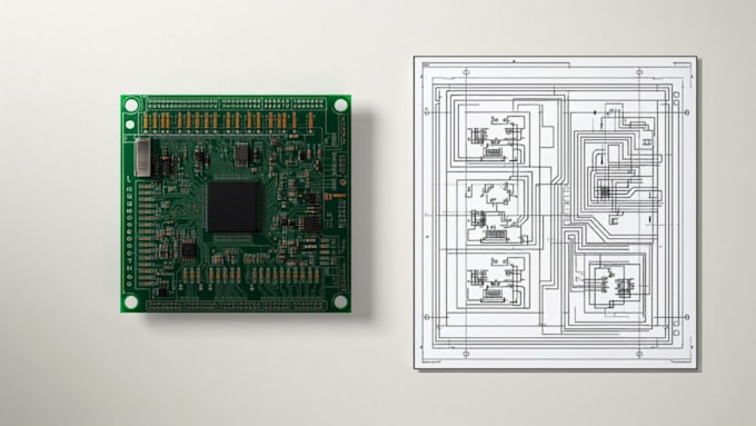
PCB design errors can cause failed prototypes, costly rework, and production delays.
I provide custom PCB deslgn, PCB layout, schematic, and circuit deslgn for your requirements. Each PCB deslgn is checked for connections, component placement, routing, and DRC issues.
WHAT I OFFER:
WHY CHOOSE ME:
I can work from your schematic, circuit diagram, reference board, datasheet, or project brief.
Need custom PCB design for your project?
Send me a message before ordering to discuss your requirements.
Specialization:
Circuit design
•
Schematics
•
Layout
File format:
Gerber
•
STEP
•
BRD
•
SCH
•
3DS
Software:
Altium Designer
•
Eagle CAD
•
KiCad
•
Matlab
•
Simulink
•
Arduino
What do you need from me to start the PCB design?
Send your schematic, circuit diagram, component list, datasheets, board dimensions, layer requirements, and preferred software (KiCad or Altium). If you only have an idea, message me first.
Can you handle a PCB project that doesn't fit your packages?
Yes. Custom PCB projects are welcome. Send your component count, layers, board size, required files, and design requirements so I can recommend the correct package or create a custom offer.
What if I need changes after the PCB layout is completed?
Revisions are included according to your selected package. I can adjust the PCB schematic, component placement, routing, or other agreed design details based on your feedback.
Will my PCB files and project information remain confidential?
Yes. Your schematics, PCB layouts, Gerber files, BOMs, datasheets, and other project assets are treated as confidential and used only to complete your order.
Can you provide Gerber files and source files?
Yes. Depending on your package, I can provide Gerber files, PCB source files, schematics, BOMs, and other agreed project deliverables for manufacturing or future editing.
Should I message you before placing a PCB design order?
Yes, especially for complex circuit design, multi layer PCB layout, or custom requirements. Send your project details first so I can confirm the scope, files, delivery time, and package.